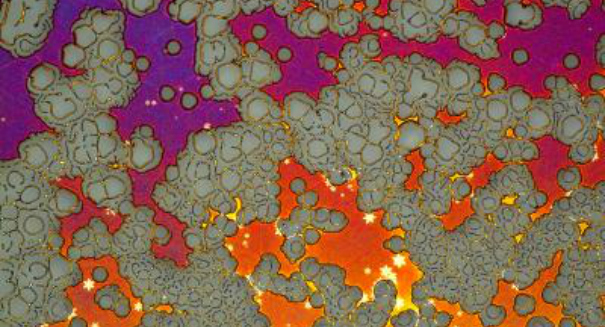
They found that large grains of copper improve the growth of the one-atom thick carbon-based material.
The American Institute of Physics reports that researchers have developed a promising new substrate recipe for the world’s strongest, thinnest material, also known as graphene. They found that large grains of copper improve the growth of the one-atom thick carbon-based material.
Giddy researchers love daydreaming about the game-changing promise of graphene-based electronics. They contend that these particular electronics could lead to faster internet speeds, less expensive solar cells and new sensors among other advancements. The appeal of graphene is that it’s light, flexible and able to conduct electricity as well as copper.
According to the American Institute of Physics, researchers at the National Institute of Standards and Technology may be on the verge of realizing graphene’s promise. While searching for the perfect growth platform for the one-atom thick carbon-based material, researchers created an interesting new formula for a graphene substrate: a thin film of copper with huge crystalline grains.
The important advancement is the grain size of the copper substrate. The huge grains are several centimeters in size, but their relative mass gives them the ability to survive the extreme temperatures vital to graphene formation.
The incapability of most copper films to survive this stage of graphene formation “has been one problem preventing wafer-scale production of graphene devices,” posited NIST researcher Mark Keller.
Thin films are a key part of many electronic, optical and medical technologies, but the grains in these films are typically smaller than one mircrometer. The researchers created a two-step process to construct the new copper substrate, whose grains are about 10,000 times bigger.
First, they positioned copper onto a sapphire wafer maintained a little above room temperature. Second, they added the transformative step of heat-treating the film at a much higher temperature, near the melting point of copper. Using this two-step process, they successfully formed graphene grains 0.2 millimeters in diameter on the new copper surface.
Read more about the research in the journal AIP Advances.
Leave a Reply