The scientists "painted" the Mona Lisa on a substrate surface approximately 30 microns in width.
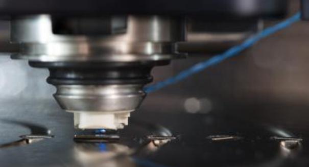
Using nanotechnology, scientists at the Georgia Institute of Technology have created the world’s smallest version of the famous Mona Lisa painting. They “painted” the Mona Lisa on a substrate surface approximately 30 microns in width. According to scientists, the method used to paint the so-called “Mini Lisa” could someday be helpful in achieving nanomanufacturing of devices because they were able to change the surface concentration of molecules on such short-length scales.
Scientists created the world’s smallest version of the Mona Lisa using an atomic force microscope and a technique called ThermoChemical NanoLithography (TCNL). To create Mini Lisa, the scientists located a heat cantilever at the substrate surface to create a series of limited nanoscale chemical reactions. By altering only the heat at each location, Keith Carroll controlled the number of new molecules that were created. More heat created Mini Lisa’s lighter shades of gray and less heat produced the painting’s darker shades of gray.
“By tuning the temperature, our team manipulated chemical reactions to yield variations in the molecular concentrations on the nanoscale,” noted lead author Jennifer Curtis, an associate professor in the School of Physics. “The spatial confinement of these reactions provides the precision required to generate complex chemical images like the Mini Lisa.”
According to the scientists, production of chemical concentration gradients and variations on the sub-micrometer scale are difficult to accomplish with other techniques. The scientists produced chemical gradients of amine groups, but believe that the method could be used with other materials.
“We envision TCNL will be capable of patterning gradients of other physical or chemical properties, such as conductivity of graphene,” Curtis said. “This technique should enable a wide range of previously inaccessible experiments and applications in fields as diverse as nanoelectronics, optoelectronics and bioengineering.”
The scientists contend that atomic force microscopes are relatively common and that the thermal control is somewhat easy to use. To help achieve their goal of nanomanufacturing devices using TCNL, the scientists have integrated nanoarrays of five thermal cantilevers to advance the pace of production.
Given that the technique exhibits high spatial resolutions at a speed much quicker than other ready-to-use methods, Curtis believes that TCNL will offer the option of nanoscale printing integrated with the fabrication of large quantities of surfaces or everyday materials whose dimensions are much larger than the TCNL features themselves.
The study’s findings are described in greater detail in the journal Langmuir.
Leave a Reply